
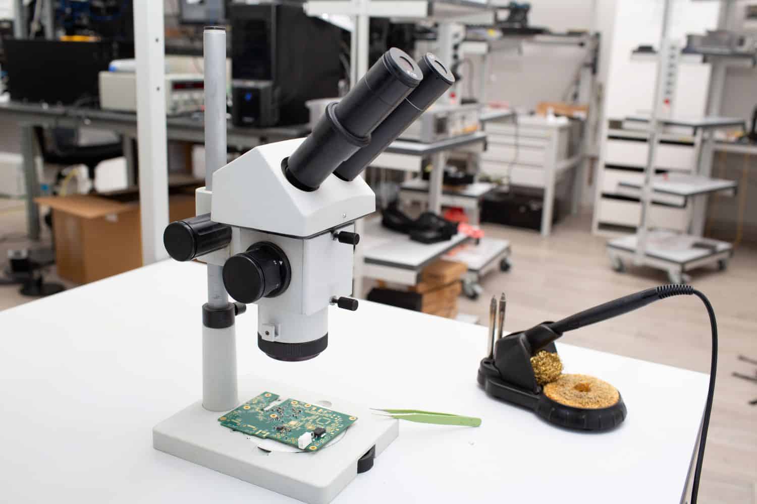
Scanning Electron Microscopy Applications Across Manufacturing Industries
While scanning electron microscopy (SEM) analysis is closely associated with automotive failure investigations, its applications extend across a wide range of manufacturing industries wherever engineers need to understand material microstructure, surface characteristics, or contamination at magnifications beyond what optical methods can achieve.
Electronics Manufacturing Applications
In electronics manufacturing, SEM analysis plays a central role in quality control and failure investigation at scales where individual solder joints, bond wires, and circuit features measure only tens of microns across. Common applications include:
- Solder joint quality assessment, examining whether solder connections show proper wetting, adequate intermetallic formation, or defects such as voiding that could compromise long-term reliability.
- Bond wire inspection, verifying that wire bonds connecting semiconductor die to package leads meet quality standards, since a poorly formed bond can lead to intermittent or complete electrical failure.
- Contamination identification on circuit boards, where SEM combined with EDX elemental analysis helps identify foreign particles that could cause short circuits or corrosion-related reliability issues.
- Package and die-level failure analysis, investigating semiconductor failures by examining die surfaces, package materials, and internal structures to determine whether a failure originated from a manufacturing defect, design issue, or field stress condition.
Metals and Materials Manufacturing
For metal fabrication and materials manufacturing broadly, SEM provides insight into microstructure that directly relates to mechanical properties and processing history:
- Grain structure analysis reveals how a metal’s microstructure relates to its mechanical properties, helping engineers understand whether heat treatment or processing achieved the intended material characteristics.
- Porosity and defect detection identifies internal voids or inclusions that could weaken a cast or machined component, often invisible through standard inspection but potentially significant to structural integrity.
- Coating thickness and adhesion evaluation examines cross-sections of coated components to verify that protective or functional coatings meet thickness specifications and show proper adhesion to the substrate material.
- Weld quality assessment inspects weld microstructure for defects such as porosity, incomplete fusion, or unwanted phase formations that could compromise joint strength.
Polymer and Composite Materials
SEM analysis also extends to polymer and composite material characterization, though these materials often require additional sample preparation consideration given their typically non-conductive nature:
- Fiber-matrix interface examination in composite materials reveals how well reinforcing fibers bond to the surrounding polymer matrix, a factor directly influencing composite mechanical performance.
- Fracture surface analysis in polymer components helps distinguish between different failure mechanisms—brittle fracture, ductile failure, or environmental stress cracking—each requiring different engineering responses.
- Filler and additive distribution assessment examines how uniformly fillers or reinforcing particles are distributed throughout a polymer matrix, since uneven distribution can create localized weak points.
Contamination and Foreign Material Investigation
Across virtually every manufacturing industry, SEM combined with EDX serves a common purpose: identifying unknown foreign material found during production or in a returned product. Whether it’s a particle causing a short circuit on a circuit board, contamination affecting a pharmaceutical product’s packaging, or debris found in a food processing environment, the same fundamental SEM-EDX approach applies—imaging the particle’s morphology and determining its elemental composition to trace its likely origin.
Why Cross-Industry Expertise Matters
Laboratories that serve multiple industries often develop broader diagnostic experience than those focused narrowly on a single sector, since failure mechanisms and contamination patterns observed in one industry can inform interpretation of similar findings elsewhere. A laboratory technician who has examined solder joint failures across both consumer electronics and automotive applications, for instance, brings pattern recognition that benefits investigations in either context.
Choosing the Right Testing Partner
For manufacturers evaluating SEM analysis providers, considerations extend beyond simply confirming the laboratory owns the appropriate equipment. Turnaround time, the availability of complementary techniques like EDX and FTIR, and the laboratory’s experience with materials and failure modes relevant to the specific industry all factor into selecting a testing partner capable of delivering not just images, but genuinely useful engineering conclusions.
Frequently Asked Questions
Does SEM analysis require different equipment for different industries?
The core SEM instrumentation remains largely consistent across applications, though sample preparation techniques and complementary analytical methods may vary depending on the material type and specific information needed for a given industry’s typical investigation questions.
How does SEM-EDX foreign material identification actually trace a contamination source?
By determining the elemental or compositional signature of an unknown particle, investigators can often compare it against known materials present in the manufacturing environment—process chemicals, equipment components, or packaging materials—to identify likely contamination sources, though confirming the exact source usually requires additional process investigation.
Can SEM analysis be used for competitor product benchmarking?
Yes, this is a legitimate application in some industries, where SEM and complementary techniques help engineers understand competitor material choices, manufacturing approaches, or component construction, informing their own product development decisions.
Is SEM analysis cost-effective for smaller manufacturers?
Given that SEM instrumentation represents significant capital investment, most smaller manufacturers rely on third-party laboratory services rather than in-house capability, making access to a well-equipped external laboratory a practical and cost-effective way to access this analytical capability without the associated equipment investment.
SEM Analysis Services in Malaysia
Malaysia’s diverse manufacturing base—spanning electronics, automotive components, and materials production—benefits from access to SEM analysis capability serving multiple industries under one accredited laboratory.
Alstesting Laboratory Testing service in Malaysia provides SEM and EDX analysis supporting failure investigation and materials characterization across electronics, automotive, and general manufacturing applications. Companies requiring scanning electron microscopy analysis for quality investigations across diverse material types gain access to broad diagnostic experience applicable well beyond any single industry sector.